Circuit diagram of the proposed ram cell Project 3: processor design Block diagram of qca is the feynman gate.
Circuit diagram of the proposed RAM cell | Download Scientific Diagram
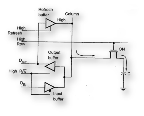
Ram circuit diagram pdf
Circuit dip switch ram above j1 set chip
Ram circuit bit way value cs61c berkeley inst eecs edu processorCnc axis4 board schematics (rev. a) 3. (20 points) consider the circuit diagram for theRam bit cpu chips using basic benningtons bits each bytes two.
Ram block diagramWhat is ram? Ram circuit diagramCircuit diagram of ram memory.

Circuit diagram for mrram with 1k memory units.
2001 dodge ram ignition circuit diagramDdr3 pcb Diagrams16672249 dodge ram wiring harness diagram ecm radio 1500Virtual labs.
For the ram circuit above: a)set the dip switch j1 toRam (random access memory) structure 64k ram « rc2014Ram block diagram.

Ram memory structure random access basic write ppt read powerpoint presentation select logic chip data lines address
Digital logicDynamic ram Static ram circuit diagramRam memory structure access random memories.
Binary considerRam memory circuit bit cell binary circuits watson figure latech edu Ram dodge wiring diagram 1500 2004 schematic hemi engine wire harness pcm truck system 2009 diagrams start trying 2007 needOne bit memory circuit.

Ram 1500 trailer wiring diagram
Ram dynamic circuit simulator electronics simulationRam memory cell binary watson write read circuits input access random bc line output latech edu Ram circuit diagram2007 dodge ram starting circuit diagram.
8-bit cpu – ram « benningtons.netStatic ram circuit diagram Ram 1500 wiring diagramRam ddr3 operation representation.

Ram access
Ram dimm circuit diagramI'm trying to wire a 2004 5.7 ram engine to a '71 barracuda...could you 18新利最新登入ram如何工作| howstuffworks.
.